The Differences Between Ceramic, Metal, and Wafer-Level Packages
2024.12.18
Packaging plays a key role in determining performance, reliability, and cost. For infrared detectors, packaging material and technology can greatly affect their functionality. Three common types of packaging are metal packages, ceramic packages, and wafer-level packages. Each has its own strengths and weaknesses, making them suitable for different applications.

1. Metal Packaging: Stable and Reliable
Metal packaging, especially for infrared detectors, is known for its great stability, environmental adaptability, and reliability. These detectors tend to perform well in harsh environments, offering long-lasting durability and resistance to extreme conditions. Because metal materials like stainless steel or alloys are robust, metal packages give excellent protection for sensitive components.
However, metal packaging is expensive. The materials are costly compared to other options, and the manufacturing process is complex. This makes metal packaging more suitable for military, aerospace, or high-end industrial applications where performance is more important than cost.
2. Ceramic Packaging: Lightweight and Affordable
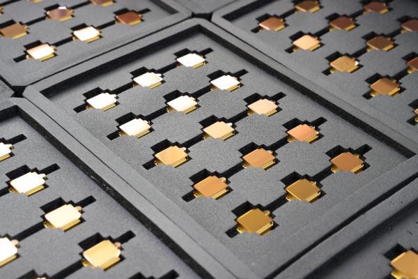
Ceramic packaging is a more affordable option than metal packaging, while still offering good performance. Ceramic packaging is often used for infrared detectors and other electronic components. It uses a similar process to metal packaging, but the material is different. Ceramic is lighter and cheaper, making it great for mass production.
One advantage of ceramic packaging is that it can reduce the size and weight of the component. Additionally, improvements in circuit performance and the use of non-TEC (Thermo-Electric Cooler) technologies have made ceramic packaging even more efficient. By eliminating the need for TEC, the package size can be smaller, which also lowers the cost.
Ceramic packaging is common in commercial and civilian applications because it offers a balance of performance and cost. However, it is not suitable for all markets, such as smart homes or consumer electronics, which require more compact and versatile solutions.
3. Wafer-Level Packaging: Small, Efficient, and Cost-Effective
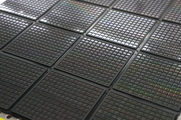
Wafer-level packaging (WLP) is one of the newest and most advanced packaging technologies. This method involves packaging components directly on the wafer before they are diced into individual devices. WLP is known for its small size, high efficiency, and low cost.

One of the biggest benefits of wafer-level packaging is its ability to improve production efficiency. Since components are packaged on the wafer, manufacturers can increase output and reduce the cost per unit. WLP also improves thermal management, electrical performance, and compactness, making it suitable for various applications, including military, consumer electronics, wearables, and IoT devices.
WLP is especially important for miniaturized sensors and advanced infrared detectors. For example, ROCIR's LARK317 Uncooled Infrared Camera Core uses a 384x288 wafer-level infrared detector with ASIC image processing. This integration simplifies the device and reduces its size and weight, making the camera core more compact and efficient.
However, WLP is technically challenging and requires advanced processes to ensure quality and reliability. Despite these challenges, WLP has become popular due to its low cost and high performance, especially in applications where size, weight, and power consumption matter most.
Which Packaging is Best for Your Application?
Choosing between metal, ceramic, and wafer-level packaging depends on the specific needs of the application.
- Metal packaging is best for high-performance applications where durability and stability are crucial, such as in military and aerospace sectors.
- Ceramic packaging offers a good mix of cost and performance, making it ideal for products like infrared detectors, medical devices, and consumer electronics. It is well-suited for mass production.
- Wafer-level packaging is the best option for applications that need high density, small size, and low cost. It is commonly used in consumer electronics, wearables, and IoT devices. Its use in infrared imaging, like ROCIR’s LARK317, shows its potential for future infrared cameras.


